

Julio César Vázquez, Ph.D.
Julio César Vázquez is a highly skilled and experienced engineer, with a strong focus on technological innovation and problem-solving. His expertise lies in the design of electronic systems hardware, with a particular emphasis on Digital Integrated Circuit (IC) design.
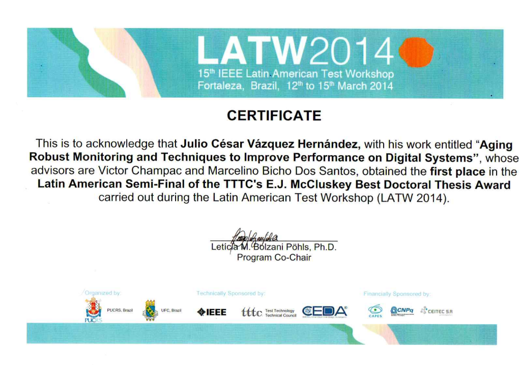
Dr. Vázquez earned his Ph.D. and Master's degrees in Science from the National Institute of Astrophysics, Optics, and Electronics (INAOE). His specialization is in VLSI (Very Large Scale Integration) Integrated Circuit Design. His doctoral thesis received significant recognition, being awarded by an international committee of experts in IC design and testing as the best doctoral thesis at the Latin-American Test Workshop held in Fortaleza, Brazil, in 2014.
He has authored multiple scientific articles published in international journals and conferences.
Throughout his master's and doctoral studies, as well as his involvement in the industry, he has gained extensive experience in the following areas
- VLSI Design and Test He employed the pre-silicon VLSI design flow to design digital structures, validate them both functionally and temporally, and apply the performance optimization proposals developed in his doctoral thesis.
- Electronic System Design: He has designed analog, digital, and mixed electronic systems.
- Embedded Systems: He has developed embedded firmware for microcontroller-based designs
- Internet of Things (IoT) He has developed solutions that integrate and communicate various IoT technology devices
His contributions to scientific research and industrial practical applications demonstrate his capability to drive technological advancements and solve complex engineering problems.
Relevant Skills

VLSI Desing and Verification
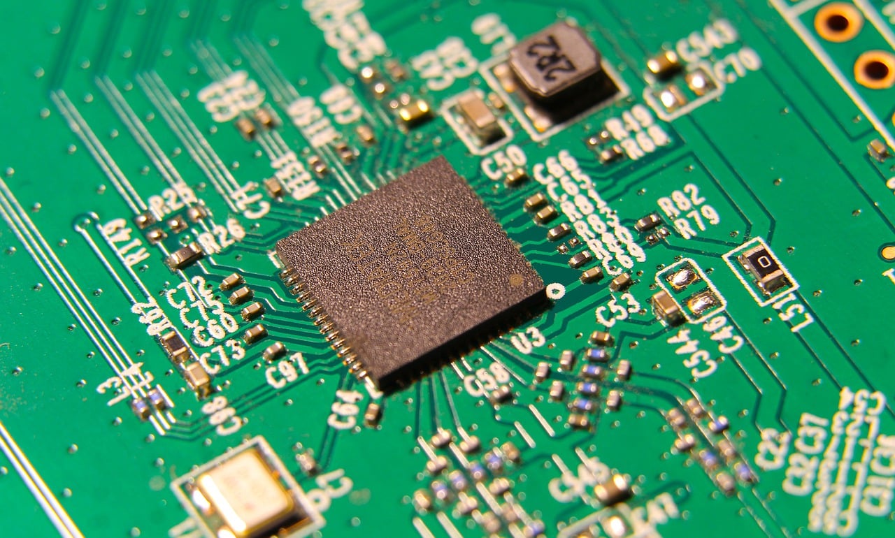
Hardware Design

Firmware Design
Courses Undertaken
As part of the ongoing professional development essential for an engineer specializing in technological innovation, several courses have been undertaken to enhance and update key competencies. Below is a list of the most relevant courses, completed through virtual platforms, which have significantly contributed to the strengthening of the professional profile.
- Electronic Circuit Design:
- Embedded Systems:
- Internet of Things (IoT)
- Artificial Intelligence and Machine Learning:
- Automotive:
Scientific Magazines and Journals

1. Process Variations-Aware Statistical Analysis Framework for Aging Sensor Insertion
Abstract: As process technology continues to shrink, Process Variations and Aging effects have an increasing impact on the reliability and performance of manufactured circuits. Aging effects produce performance degradation as time progresses. This degradation rate depends on: a) Operational conditions and b) Static technological parameters defined in the fabrication process. Moreover, performance of electronic systems for safety-critical applications which operate for many years in harsh environments are more prompt to be impacted by aging. In order to guarantee a safe operation in advanced technologies, aging monitoring should be performed on chip using built-in aging sensors. The purpose of this work is to present a methodology to determine the correct location for aging sensor insertion, considering the combined impact of process variations (PV) and aging effects. In order to implement the methodology a path-based Statistical Timing Analysis framework and tools have been developed. It is shown that delay path reordering, asssociated with PV and Aging, may justify the insertion of a few aditional sensors to cover abnormal delays of signal paths that become critical under long system operation
2. Delay sensing for long-term variations and defects monitoring in safety-critical applications
Abstract: The impact of parametric variations on digital circuit performance is increasing in nanometer Integrated Circuits (IC), namely of Process, power supply Voltage and Temperature (PVT) variations. Moreover, circuit aging also impacts circuit performance, especially due to Negative Bias Temperature Instability (NBTI) effect. A growing number of physical defects manifest themselves as delay faults (at production, or during product lifetime). On-chip, on-line delay monitoring, as a circuit failure prediction technique, can be an attractive solution to guarantee correct operation in safety–critical applications. Safe operation can be monitored, by predictive delay fault detection. A delay monitoring methodology and a novel delay sensor (to be selectively inserted in key locations in the design and to be activated according to user’s requirements) is proposed, and a 65 nm design is presented. The proposed sensor is programmable, allowing delay monitoring for a wide range of delay values, and has been optimized to exhibit low sensitivity to PVT and aging-induced variations. Two MOSFET models—BPTM and ST—have been used. As abnormal delays can be monitored, regardless of their origin, both parametric variations and physical defects impact on circuit performance can be identified. Simulation results show that the sensor is effective in identifying such abnormal delays, due to NBTI-induced aging and to resistive open defects.

3. Testing of Stuck Open Faults in Nanometer Technologies
Abstract: Opens have become an important defect mechanism in modern technologies. An open defect type of significant concern is called the CMOS stuck-open fault (SOF). SOF are dificult to test because they require at least a two-vector sequence. Unfortunately, test detection of this defect is made by chance: either from a lucky sequence of vectors in a functional, stuck at fault, or delay fault voltage-based test set, or by chance in an IDDQ test. Failure analysis can experience seemingly contradictory measurements making the analysis frustrating. The presence of SOFs may make some transition faults invalid. This paper shows how ICs implemented in technologies having low-signal-node capacitance that interact with transsitor leakage currents can alter classic SOF behavior, which presens an even more complex detection challenge. The results show that leakage currents in SOF output nodes introduce more variables that further complcate detection. Results also show that normal IC noise may introduce a noisy output response that may or may not be correct.
International Conferences:

4. Programmable Aging Sensor for Automotive Safety-Critical Applications
Abstract: Electronic systems for safety-critical automotive applications must operate for many years in harsh environments. Reliability issues are worsening with device scaling down, while performance and quality requirements are increasing. One of the key reliability issues is long-term performance degradation due to aging. For safe operation, aging monitoring should be performed on chip, namely using built-in aging sensors (activated from time to time). The purpose of this paper is to present a novel programmable nanometer aging sensor. The proposed aging sensor allows several levels of circuit failure prediction and exhibits low sensitivity to PVT (Process, power supply Voltage and Temperature) variations. Simulation results with a 65 nm sensor design are presented, that ascertain the usefulness of the proposed solution.

5. Low Sensitivity to Process Variations Aging Sensor for Automotive Safety Critical Applications
Abstract: In this paper, circuit failure prediction by timing degradation is used to monitor semiconductor aging, which is a safety-critical problem in the automotive market. Reliability and variability issues are worsening with device scaling down. For safe operation, we propose on-chip, on-line aging monitoring. A novel aging sensor (to be selectively inserted in key locations in the design and to be activated from time to time) is proposed. The aging sensor is a programmable delay sensor, allowing decision-making for several degrees of severity in the aging process. It detects abnormal delays, regardless of their origin. Hence, it can uncover normal aging (namely, due to NBTI) and delay faults due to physical defects activated by long circuit operation. The proposed aging sensor has been optimized to exhibit low sensitivity to PVT (Process, power supply Voltage and Temperature) variations. Simulation results with a 65 nm sensor design are presented, ascertaining its usefulness and its low sensitivity, in particular to process variations.

6. Stuck-Open Fault Leakage and Testing in Nanometer Technologies
Abstract: The stuck-open fault (SOF) is a difficult, hard failure mechanism unique to CMOS technology. Its detection requires a specific 2-vector pair that examines each transistor in the logic gate for an open defect in its drain and/or source. In this work it is shown that this failure mechanism is very alive and relevant to modern technologies. The small nanometer technology capacitances and the increased leakage currents result in faster discharges of the floating high impedance node making fault detection more difficult. A test vector strategy is proposed to improve the detection of this fault for technologies with gate current leakage.
Oral Presentations in International Conferences
1. Aging Robust Monitoring and techniques to improve Performance on Digital Systems

Abstract: As process technology continues to shrink, Process Variations and Aging effects have an increasing impact on the reliability and performance of manufactured circuits. Aging effects produce performance degradation as time progresses. This degradation rate depends on: a) Operational conditions and b) Static technological parameters defined in the fabrication process. Moreover, performance of electronic systems for safety-critical applications which operate for many years in harsh environments are more prompt to be impacted by aging. In order to guarantee a safe operation in advanced technologies, aging monitoring should be performed on chip using built-in aging sensors. The purpose of this work is to present a methodology to determine the correct location for aging sensor insertion, considering the combined impact of process variations (PV) and aging effects. In order to implement the methodology a path-based Statistical Timing Analysis framework and tools have been developed. It is shown that delay path reordering, asssociated with PV and Aging, may justify the insertion of a few aditional sensors to cover abnormal delays of signal paths that become critical under long system operation.
In this Workshoop Julio Cesar Vazquez has presented his main important PhD disertation results. After evaluating all the PhD disertations, submited in this workshoop, an expert evaluators commitee decided to award this disertation as the best doctoral thesis.
En este taller, Julio César Vázquez presentó los resultados más importantes de su tesis doctoral. Después de evaluar todas las tesis doctorales presentadas en este taller, un comité de evaluadores expertos decidió otorgar a esta disertación el premio a la mejor tesis doctoral.
The certificate of this award is shown below:
2. Low Sensitivity to Process Variations Aging Sensor for Automotive Safety Critical Applications

This paper was submited in the «VLSI Test Symposium» and also was selected as oral presentation. Therefore this paper is also included here. The abstract of this paper can be shown in 5th article position of the above section.
Oral Presentations in Universities
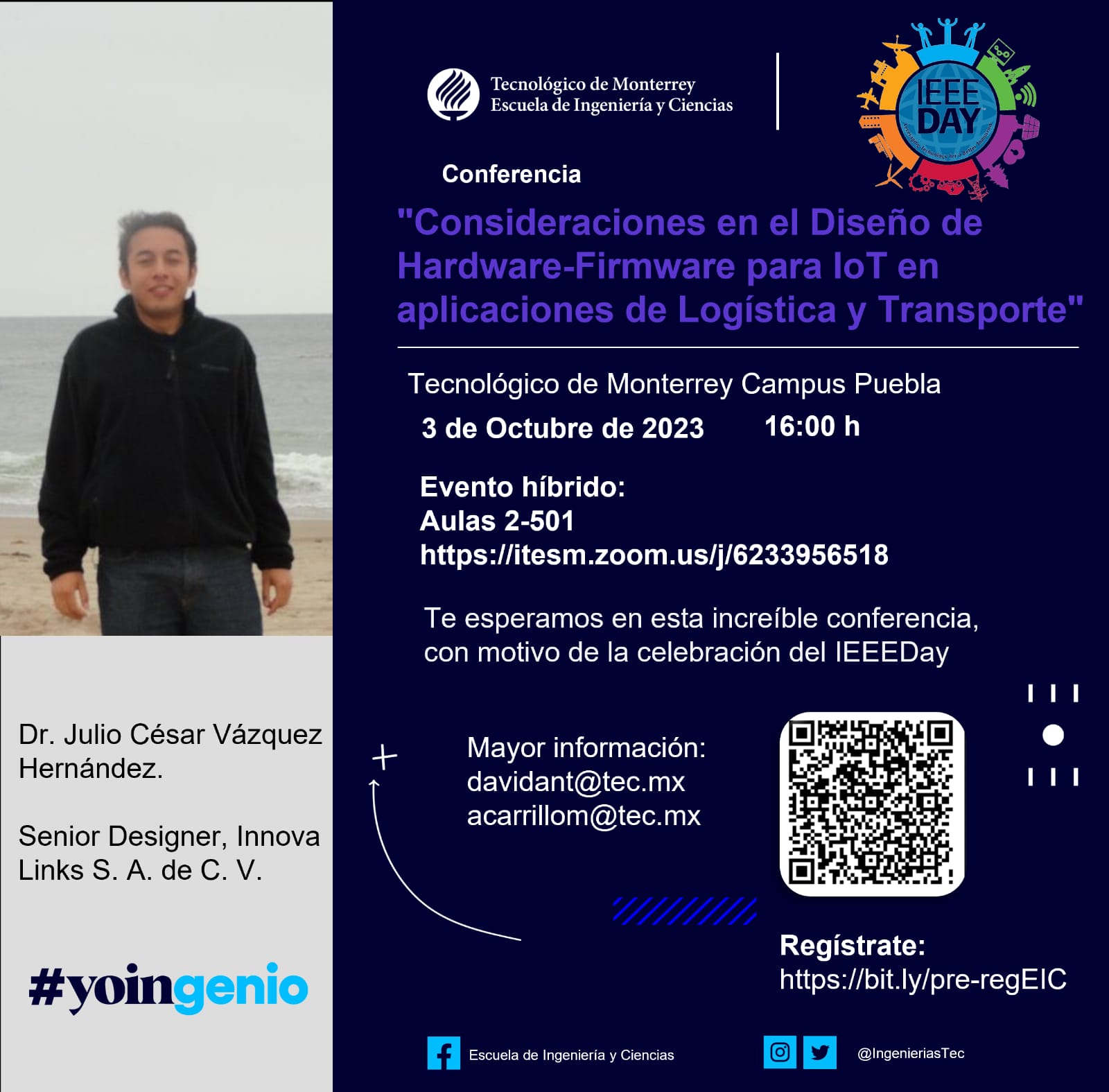
Hardware-Firmware Design Considerations for IoT in Logistics and Transportation Applications
Abstract: This lecture was given at the Tecnológico de Monterrey, Puebla campus. It covered the most important aspects that must be taken into account when designing Internet of Things (IoT) systems applied to the Logistics and Transportation industry.
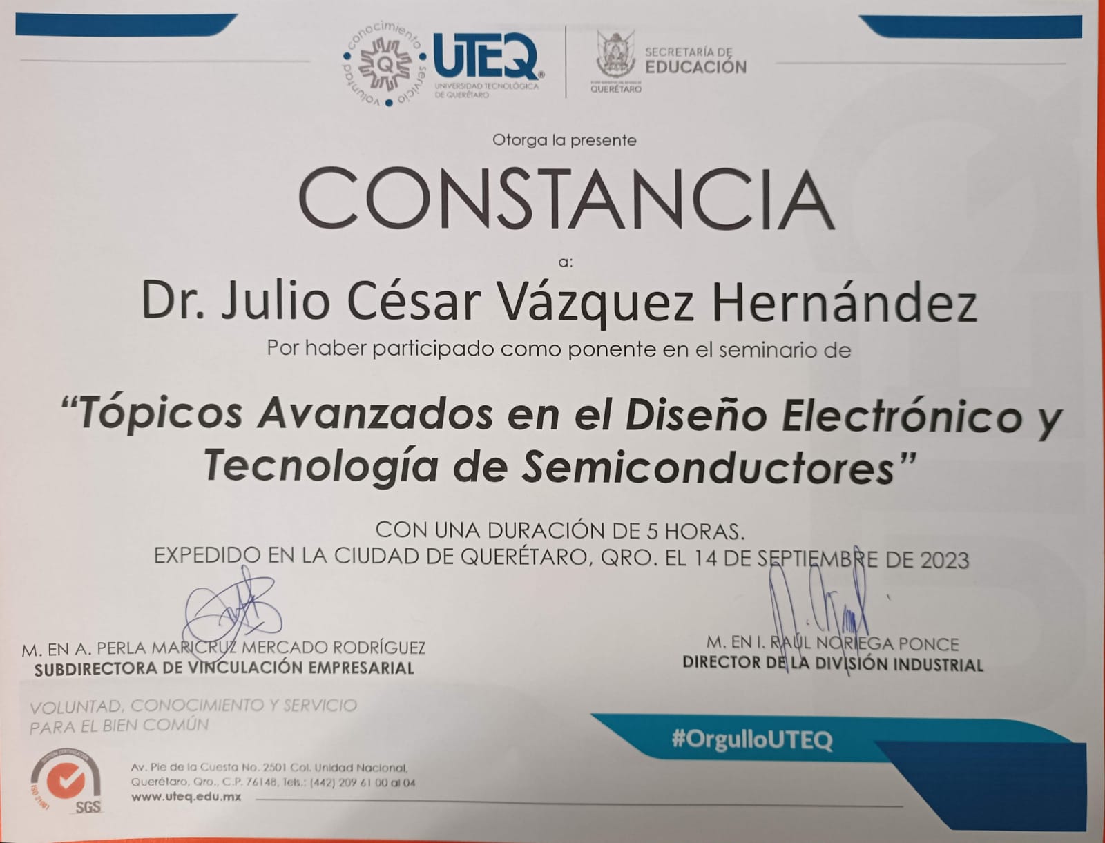
Advanced Topics in Electronic Design and Semiconductor Technology.
Abstract: This seminar was given at the Technological University of Querétaro. It discussed the considerations to be taken into account when developing microcontroller-based electronic systems. Best practices were presented in: a) hardware design, specifically when designing voltage regulators, and b) firmware design for microcontroller-governed systems.