Ph. D. Degree
Integrated Circuit, VLSI Design
Thesis: Aging Robust Monitoring and techniques to improve Performance on Digital Systems.
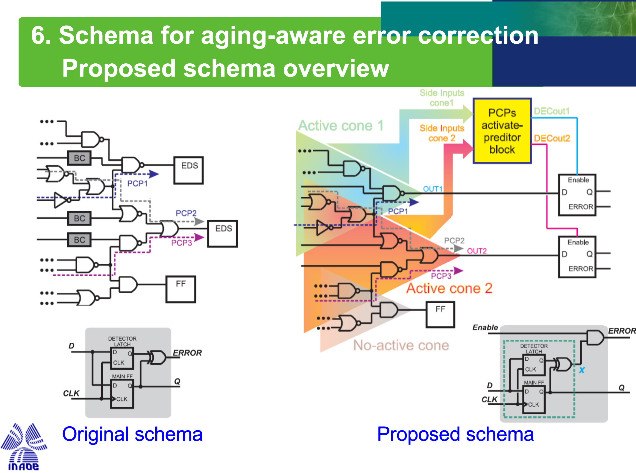
In order to ensure reliable operation in advanced technologies, aging monitoring must be developed within the chip using built-in aging sensors. The main methods to develop such aging monitoring are classified into two groups: a) Error Prediction and b) Error Correction. In this thesis, various methodologies and schemes will be proposed to achieve robust aging monitoring for error prediction and correction in nanometric digital integrated circuits.

As technological scaling has progressed, aging effects such as Negative Bias Temperature Instability (NBTI) have become of utmost importance in nanometric CMOS technologies. On the other hand, the impact of parametric variations has further exacerbated these effects. Process, Voltage, Temperature, and Aging variations (PVTA) have a strong impact on the reliability and performance of integrated circuits in operation. NBTI-induced aging causes performance degradation as the operation time increases. The rate of this degradation depends on: a) the operational conditions experienced by the circuits, such as Voltage, Temperature, and the electrical stress time of MOS transistors, and b) the static technological parameters defined in the fabrication process.

M.Sc. Degree
Integrated Circuit, VLSI Design
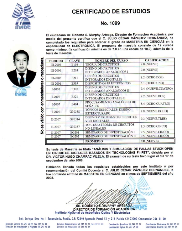
Thesis: Analysis and simulation of Stuck-Open Faults in Digital Circuits based on FinFET technologies
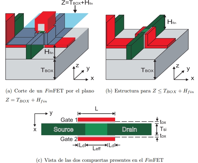
VLSI integrated circuit design has been based on the MOSFET device for the past three decades. However, scaling down the MOSFET to the nanometer regime presents some undesirable effects that degrade the performance of this device. One option to continue technological scaling beyond 32nm is the use of new structures, such as double-gate transistors (DGMOSFETs), which find the most suitable way to be fabricated in the FinFET. The International Technology Roadmap for Semiconductors (ITRS) recognizes the importance of these devices in future technologies.

The FinFET belongs to the family of devices based on Silicon-on-Insulator technologies. It is a fin-shaped device, which is surrounded by a gate electrode forming two properly aligned channels on the vertical walls of the fin. Stuck-open faults have traditionally been recognized as difficult to detect in technologies mainly because they require a sequence of vectors for their detection. As future technologies increase the density of devices, the number of metals, and the number of vias, there will be a higher probability of having stuck-open faults. This work focuses on the study of stuck-open faults in static CMOS gates based on FinFET technologies. Furthermore, this work aims to determine how leakage currents in FinFETs affect the behavior of digital gates under test.

Electronic Engineering
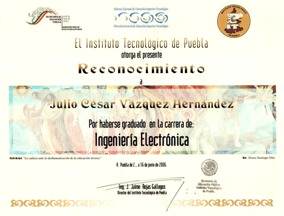
The engineering program was completed at the Instituto Tecnológico de Puebla. The engineering degree was automatically awarded for achieving an average grade of 90/100 in the program's courses. Some of the most important courses that were completed in this engineering program are:
a) Analog Electronic Systems
b) Digital Electronic Systems
c) Microcontrollers
d) Control Systems
e) Instrumentation
f) PLCs
g) Robotics
